


Top story

Samsung Galaxy Unpacked 2022
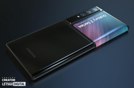
Samsung Unpacked 2022: Galaxy Z Fold 4 en Galaxy Z Flip 4
Samsung bevestigt de datum voor het Galaxy Unpacked 2022 launch event, waar de Z Fold 4 en Z Flip 4 vouwtelefoons worden verwacht. ...